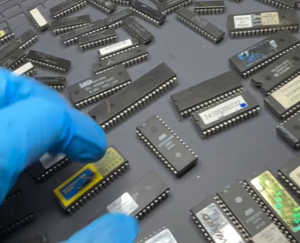
Integrated chip under microscope
Meta Title: Integrated Chips Under a Microscope: Revealing the Hidden Marvels of Microelectronics
Meta Description: Discover how an integrated chip looks under a microscope! Learn about its intricate structure, manufacturing details, and the technology behind microscopic analysis.
Zooming In: The Fascinating World of Integrated Chips Under a Microscope
Integrated chips (ICs) are the unsung heroes of modern electronics, powering everything from smartphones to spacecraft. Yet to the naked eye, these tiny silicon slivers appear as little more than glossy black rectangles with metallic pins. The real magic lies beneath the surface—revealed only when an integrated chip is placed under a microscope.
In this article, we’ll explore how microscopy unlocks the hidden architecture of ICs, why this inspection is critical for innovation, and what the stunning visuals tell us about the future of microelectronics.
Why Microscopic Inspection of Integrated Chips Matters
Microscopy isn’t just about curiosity—it’s a cornerstone of semiconductor research, quality control, and failure analysis. Here’s why peering at chips at micrometer or nanometer scales is indispensable:
- Quality Assurance: Detecting defects like cracks, misalignments, or impurities during manufacturing.
- Reverse Engineering: Understanding competitors’ designs or diagnosing obsolete chips.
- Research & Development: Optimizing transistor density,新材料, or energy efficiency.
- Failure Analysis: Identifying root causes of chip malfunctions (e.g., overheating, electromigration).
Inside an Integrated Chip: Key Structures Revealed Under Magnification
When observed under high-powered microscopes, an IC transforms into a labyrinth of layered circuits. Here’s what you’ll see:
1. Transistors (The Building Blocks)
Billions of transistors—often FinFETs or GAAFETs in cutting-edge chips—appear as intricate 3D structures. These switches control electrical currents and form the logic gates behind computing.
2. Interconnects (The “Wiring”)
A web of copper or aluminum interconnects links transistors. Microscopy reveals multilayer metallization, with each layer insulated by dielectrics like silicon dioxide.
3. Bonding Wires & Pads
Gold or copper wires connect the chip’s core to its external pins. Under magnification, these delicate threads highlight precision soldering techniques.
4. Doping Regions
Chemical alterations (doping) create semiconductor properties. Advanced microscopy can map doped areas using electron contrast or chemical imaging.
5. Packaging Layers
Protective coatings, heat spreaders, and solder bumps become visible, showcasing how chips withstand mechanical stress and thermal cycles.
Types of Microscopes Used in IC Analysis
Different goals demand different tools. Here’s how engineers and scientists inspect chips:
| Microscope Type | Key Features | Use Cases |
|---|---|---|
| Optical Microscope | Up to 2000x magnification; color imaging. | Initial defect checks, bond wire inspection. |
| Scanning Electron Microscope (SEM) | 1,000,000x magnification; 3D surface imaging. | Detailed topology, fracture analysis. |
| Transmission Electron Microscope (TEM) | Atomic-level resolution; cross-sectional views. | Transistor gate measurements, material crystallography. |
| Atomic Force Microscope (AFM) | Measures surface roughness at nanoscale. | Profiling thin films, detecting voids. |
Applications of IC Microscopy in Industry
1. Failure Analysis Labs
SEM and TEM help diagnose dead chips by locating burnt traces, electrostatic discharge damage, or corrosion.
2. Semiconductor Manufacturing
In-line microscopes monitor fabrication processes like lithography and etching in real-time.
3. Reverse Engineering
Delaminating chips layer by layer (e.g., with plasma etching) allows engineers to reconstruct circuit blueprints.
4. Academic Research
Universities use microscopy to experiment with novel materials (e.g., graphene transistors) or quantum computing components.
A Step-by-Step Guide to Imaging an Integrated Chip
Want to try it yourself? Here’s a simplified workflow:
-
Sample Preparation
- Decapsulation: Remove epoxy packaging using acid etching or laser ablation.
- Polishing: Create a smooth cross-section for TEM/SEM viewing.
-
Microscope Selection
Start with optical microscopy for an overview, then switch to SEM/TEM for nanoscale details. -
Imaging Parameters
Adjust voltage, beam current, and detectors (e.g., backscattered electrons for material contrast). -
Analysis Software
Tools like ImageJ or Gwyddion measure feature sizes, layer thickness, and defect densities.
The Future of IC Microscopy: AI, Automation & Beyond
Emerging trends are revolutionizing how we study chips:
- AI-Powered Defect Detection: Machine learning algorithms scan thousands of images to flag anomalies faster than humans.
- In Situ Microscopy: Observing chips under real operating conditions (e.g., during electrical load).
- 3D Tomography: X-ray microscopes generate non-destructive 3D models of stacked chips (e.g., in HBM memory).
Conclusion: Where Art Meets Engineering
Viewing an integrated chip under a microscope isn’t just scientific—it’s awe-inspiring. The geometric perfection of nanometer-scale circuits is a testament to decades of human ingenuity. As transistors shrink toward atomic limits, microscopy remains our window into this microscopic universe, driving innovations that will redefine technology.
Call to Action:
Curious about how microscope imagery shapes chip design? Share your thoughts below or explore our deep-dive into [semiconductor manufacturing processes]!
Keywords: Integrated chip under microscope, IC microscopy, SEM analysis, semiconductor inspection, microchip structure, failure analysis, reverse engineering.


